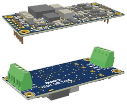
BD Family of Dual Channel Drivers
for Piezo Bender Actuators
Piezoelectric Drivers
 BD Specifications
 Calculate Power Bandwidth
The BD family of miniature driver modules contain a high-voltage power supply and two linear amplifier channels. The individual channels can drive piezoelectric actuators up to +300V, or can be combined for a single output up to +/-300V. An inverting option allows these modules to drive two and three wire piezoelectric bender actuators.
The 3V input range, fast response, and high peak current suits applications including high speed valves, robot actuators, non-resonant piezo motors, and motion control applications.
The BD family of modules include comprehensive overload protection and are available with screw terminals or PCB mounting pins.
Voltage Ranges
| Variant | Output Voltage | Differential Output | Gain | Peak Current | RMS Current |
|---|---|---|---|---|---|
| BD300 | 300V | +/-300V | 101 | 50 mA | 11 mA |
| BD250 | 250V | +/-250V | 83.6 | 59 mA | 13 mA |
| BD200 | 200V | +/-200V | 67.7 | 73 mA | 16 mA |
| BD150 | 150V | +/-150V | 51.0 | 95 mA | 21 mA |
Operation:
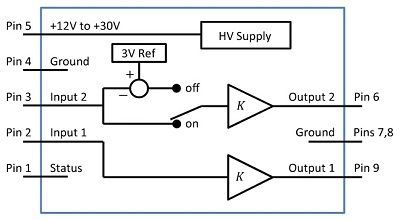
The modules contain a high voltage DC-DC converter and two linear amplifier channels. A range of maximum output voltages are available, from +150V to +300V. The minimum output voltage is approximately +3V, which is due to the push-pull output circuit that cannot reach exactly zero volts.
Since the minimum output is limited to approximately +3V, the minimum useful input voltage is approximately +3V/Gain. For example, the minimum useful input voltage of the BD300 is 300V/101 = 30 mV. For simplicity, this limitation is not considered in the following application examples.
Channel 2 can be switched between a non-inverting configuration (on) which is identical to channel 1, or an inverting configuration (off), which is useful when driving three wire benders or creating a single differential output.
Application Example: Independent Channels
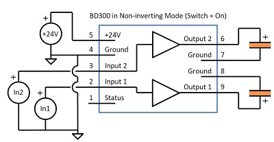
In this example, two 0V to 3V input signal sources produce a 0V to full-range output on two independent loads. It is recommended to connect the power supply directly to Pin 5 and 4 via twisted pair cable (if using screw terminals).
Application Example: +/-200V Piezo Driver
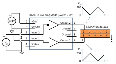
This example shows a series poled bender driven in the “two-wire” configuration [1]. A 0V to 3V input signal produces +/-200V output. Note that the load is driven differentially and cannot be connected to ground. Channel 2 is configured in the inverting mode by setting the switch to “off”. The voltage at output 1 is V1=KVin , and the voltage at output 2 is V2=K(3-Vin) , where K=67.7 for the BD200. Therefore, the voltage across the load is VLOAD = V1-V2=2K(Vin-1.5)
Therefore, a 0V input produces -200V across the load, 1.5V input produces 0V across the load, and 3V produces +200V across the load. When the output voltage is positive, the actuator bends downward.
The deflection δ is δ = 2K(Vin-1.5) δpp/Vpp
where δpp is the peak-to-peak displacement of the bender, and Vpp is the maximum peak-to-peak voltage. For example, δpp=1.048mm, and Vpp = 360 for the T220-A4BR-2513XB actuator www.piezo.com.
Application Example: Three-wire Bender Driver
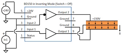
This example shows a parallel poled bender driven in the “biased unipolar” or “three-wire” configuration [1]. The +150V bias voltage is achieved by configuring channel 2 in inverting mode and grounding the input.
A zero volt input results in +150V across the top piezo layer and maximum upward deflection. A +3V input results in +150V across the bottom piezo layer and maximum downward deflection. The deflection δ can be represented by
 where δpp is the peak-to-peak displacement of the bender. Examples of compatible actuators are listed below:
| Actuator | Part Number | Bias Voltage | Amplifier |
|---|---|---|---|
 |
PiezoDrive BA6020 | +150V | BD150 |
 |
Thorlabs PB4NB2W | +150V | BD150 |
 |
Noliac CMBR02 (see note 1) | +200V | BD200 |
Note 1: The recommended +100V and -100V bias voltages can be replaced by +200V and 0V
Other Specifications
| Specification | Value | Notes |
|---|---|---|
| Input Voltage range | 0V to 3V | Minimum useful input voltage is 3V/Gain. |
| Input Impedance | 10kΩ, 5kΩ | Channel 1 is 10kΩ, Channel 2 is 5kΩ |
| Minimum output voltage | <3V | Output voltage does not reach zero |
| Over-current protection | Peak and RMS | Includes direct short circuit |
| Thermal protection | 70C | Disabled when PCB temp > 70C |
| Power Supply | +12V to +30V | +24V recommended |
| Supply power | 5 W | Maximum average power under full load |
| Small signal bandwidth | 20 kHz | |
| Slew rate | 12V/us | |
| Output noise | <1% of full range | E.g. <3 Vpp for BD300 |
| Status pin voltage | 0.6 V | <0.5V signals a thermal overload |
| Temperature range | -20 C to +50 C | |
| Humidity | Non-condensing | |
| Dimensions | 60 x 25.4 mm | 2.3 x 1 inch |
| Height | 8 mm | Total height required for PCB mount version |
| Weight | 11 g |
Output Current
The peak and average current limit specifications are listed in “Voltage Ranges”. The RMS current limit defines the maximum frequency that is achievable with a capacitive load, which is discussed in “Power Bandwidth”. The peak current can be drawn for up to five milliseconds before the RMS current limit engages. This allows fast step changes with capacitive loads. The output voltage slew rate is:
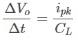
Where  is the peak current limit, CL is the load capacitance, ΔV0 is the change in output voltage, and Δt is the time interval. For example, a voltage change of ΔV will require a slewing time of
 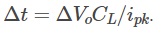 .
.
Power Bandwidth
The power bandwidth is the maximum frequency periodic signal that can be reproduced without distortion. The online power bandwidth calculator determines the maximum operating frequency and required power for a given load capacitance. The calculator includes the effects of current limit, slew-rate, and signal bandwidth.
The calculator does not include the time-constant of the peak current limit, and therefore may become inaccurate when the power bandwidth is below 50 Hz.
Calculate Power Bandwidth
Signal Bandwidth and Settling Time
With a load capacitance below 10 nF, the small signal bandwidth of the BD modules is 20 kHz. The rise-time with a step input is approximately 20 us.
With a load capacitance above 10 nF, the bandwidth and rise-time are effected by the output impedance, current limit, and voltage slew-rate. For periodic signals, refer to the online calculator above. For step-response rise times, refer to “Output Current”.
Heat Dissipation
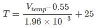
When driving capacitive loads, the heat dissipation of the module is equal to the required supply power calculated by the online calculator. The worst case is approximately 5W which may require some enclosure ventilation for passive convection. The PCB temperature can be monitored by measuring the voltage on the test point labelled “Temp”. The temperature in degrees C is
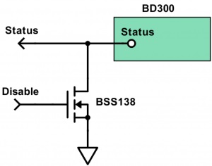
Status Pin
In normal operation, the status pin voltage is 0.6V. If the voltage drops below 0.5V, this indicates that the PCB temperature is above 70C and the power supply has been temporarily disabled. The status pin can also be pulled low to disable the high-voltage power supply. For example, by using the circuit below:
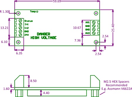
Dimensions BDxxx-Screw
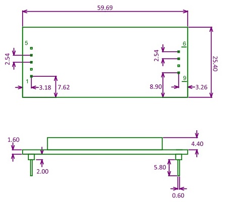
Dimensions BDxxx-PCB (mm)
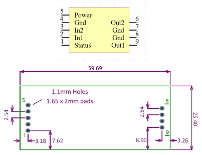
PCB Footprint
High Voltage Safety Warning
This product produces potentially lethal voltages up to 330 Vdc.
- Observe Low-Voltage (as per ANSI C84.1-1989) safety precautions, e.g.
- Use an observer trained in low-voltage rescue
- Do not operate with exposed conductors
- Use appropriate signage.
Certifications and Compliance
References
[1] A New Electrical Configuration for Improving the Range of Piezoelectric Bimorph Benders; S. A. Rios, A. J. Fleming; Sensors and Actuators A: Physical, 2015.